參考價(jià)格
面議型號
品牌
產(chǎn)地
英國樣本
暫無看了牛津Oxford原子層刻蝕機(jī)PlasmaPro 100 ALE的用戶又看了
 留言詢價(jià)

虛擬號將在 180 秒后失效
使用微信掃碼撥號
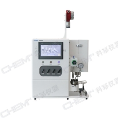
牛津Oxford原子層刻蝕機(jī) PlasmaPro 100 ALE
As layers become thinner to enable the next generation semiconductor devices there is a need for ever more precise process control to create and manipulate these layers. The PlasmaPro 100 ALE delivers this through specialised hardware including:
· Precise control of gas dose
· Excellent repeatability of low power RF delivery
· Rapid switching enabled by fast PLC
All these combine to enable etching with accuracy at the atomic scale.概述:
我們的設(shè)備和工藝已通過充分驗(yàn)證,正常運(yùn)轉(zhuǎn)時(shí)間可達(dá)90%以上,,一旦設(shè)備安裝完畢,,可立即投入使用。PlasmaPro 100系列市場應(yīng)用廣,,包括但不限于: MEMS和傳感器,、光電子、分立元器件和納米技術(shù),。它具有足夠的靈活性,,可用于研究和開發(fā),通過打造質(zhì)量滿足生產(chǎn)需求,。
PlasmaPro 100 ALE 的特點(diǎn):
· 準(zhǔn)確的刻蝕深度控制,;
· 光滑的刻蝕表面
· 低損傷工藝
· 數(shù)字化/循環(huán)式刻蝕工藝——刻蝕相當(dāng)于ALD
· 高選擇比
· 能加工**200mm的晶圓
· 高深寬比(HAR)刻蝕工藝
· 非常適于刻蝕納米級薄層
應(yīng)用:
· III-V族材料刻蝕工藝
· 固體激光器InP刻蝕
· VCSEL GaAs/AlGaAs刻蝕
· 射頻器件低損傷GaN刻蝕
· 硅 Bosch和超低溫刻蝕工藝
· 類金剛石(DLC)沉積
· 二氧化硅和石英刻蝕
· 用特殊配置的PlasmaPro FA設(shè)備進(jìn)行失效分析的干法刻蝕解剖逆工藝,可處理封裝好的芯片,, 裸晶片,,以及200mm晶圓
· 高質(zhì)量PECVD沉積的氮化硅和二氧化硅,用于光子學(xué),、電介質(zhì)層,、鈍化以及諸多其它用途
· 用于高亮度LED生產(chǎn)的硬掩模沉積和刻蝕
暫無數(shù)據(jù),!
 牛津Oxford原子層刻蝕機(jī)PlasmaPro 100 ALE的工作原理介紹,?牛津Oxford原子層刻蝕機(jī)PlasmaPro 100 ALE的使用方法,?牛津Oxford原子層刻蝕機(jī)PlasmaPro 100 ALE多少錢一臺(tái)?牛津Oxford原子層刻蝕機(jī)PlasmaPro 100 ALE使用的注意事項(xiàng)牛津Oxford原子層刻蝕機(jī)PlasmaPro 100 ALE的說明書有嗎,?牛津Oxford原子層刻蝕機(jī)PlasmaPro 100 ALE的操作規(guī)程有嗎,?牛津Oxford原子層刻蝕機(jī)PlasmaPro 100 ALE的報(bào)價(jià)含票含運(yùn)費(fèi)嗎?牛津Oxford原子層刻蝕機(jī)PlasmaPro 100 ALE有現(xiàn)貨嗎,?牛津Oxford原子層刻蝕機(jī)PlasmaPro 100 ALE包安裝嗎,?
 手機(jī)版: